January 20, 2014

Note from the Author

Hello folks!

In the last two days, I have come across many blogs which have used my content. 

While I feel glad that these guys have chosen my content to publish and I'm quite sure many people must have reaped benefits from it, it does hurt me to see the content- exactly same words (with even the same font!), same figures/pictures being used- without even acknowledging the source. I also understand that the end goal of all these people (including me) might be the same which is to enlighten the budding VLSI engineers, but I would urge these guys to at least acknowledge the source.
 
To name a few: 

In retrospect, in case anyone feels that any material on this blog is inappropriate, I would urge you to feel free to drop me a mail at my.personal.log@gmail.com and I assure you that I would take necessary action, even it if means completely obliterating the post or perhaps even the blog, at the earliest.

Thanks!

Regards,
Naman Gupta

January 18, 2014

Problem: Sequential Element

Another problem for you!

Consider the following circuit. Assume that each inverter takes 1 time unit for a low-to-high or high-to-low transition. Assume that it takes 1 time unit for a pull-up path or pull-down path to pull-up or pull-down respectively. Ignore any leakage effects. Assume VDD >> VT. Also assume that there is no skew between CLK and CLK_BAR and assume that rise/fall times on all signals are zero.


  1. What type of sequential element is the above circuit? (Hint: Plotting the X, Y and Q with respect to the waveform of CLK and D might help you in finding the answer.)
  2. What is the propagation delay of this sequential element?


Source: 
Massachusetts Institute of Technology
Dept. of Electrical Engineering and Computer Sciences
Analysis and Design of Digital Integrated Circuits- Fall 2003, Quiz #2
Prof. Anantha Chandrakasan


January 04, 2014

Problem: Energy Consumption

I came across an interesting problem and thought I would share it with you folks:
 
A battery-operated 65nm digital CMOS device is found to consume equal amounts (P) of dynamic power and leakage power while the short-circuit power is negligible. The energy consumed by a computing task, that takes T seconds, is 2PT.
 
Compare two power reduction strategies for extending the battery life:
  • Clock frequency is reduced to half, keeping all other parameters constant.
  • Supply voltage is reduced to half. This slows the gates down and forces the clock frequency to be lowered to half of its original (full voltage) value. Assume that leakage current is held unchanged by modifying the design of transistors.
Please post your answers as comments to this blog post.
 
Source: Dynamic and Static Power in CMOS. A Presentation by Vishwani D. Agrawal, Auburn University, USA and Srivaths Ravi,Texas Instruments India.
 

The Legend of Synchronizer

Long time ago, there were two warriors: Clock Domain 1 and Clock Domain 2. Each had their respective clocks CLK-1 and CLK-2 which they contended to be the master of their own will! The frequency and the phase relationship of the two clocks were independent of each other.


In absence of any such relationship, there is a possibility of the two clock edges being precariously close that could in turn cause a timing violation. The metastable output of the FF-2 could pass on to the entire system and disrupt the entire computation of the chip. FF-S steps in to resolve the impasse and urges the two clock domains to have a deterministic relationship between their clocks.


But the two clock domains refuse to budge! Neither of them were willing to curtail the freedom of their clocks which they deeply cherished! 

Here the FF-S sacrifices its own output and offers a solution to the clock domains.

That's how the FF-S ensured the prosperity of the entire SoC by suffering a metastability at it's own output. And since then it's been called The SYNCHRONIZER Flop! Note that it is necessary to connect the synchronizer flop's clock to the clock of the second domain.

Over the years, there's been a practice of using up to three such synchronizer flops depending upon the application.

I'll talk about the concept of Mean Time Before Failure (MTBF) which is very closely related to metastability shortly.

August 15, 2013

Integrated Clock and Power Gating

Clock Gating and Power Gating are two most commonly used design methods to save dynamic and leakage power respectively. How about integrating the two solutions such that they complement each other? In this post, I will talk about a simple way to do so.

Clock Gating is accomplished by using Clock Gating Integrated Cell (CGIC) which gates the clock to the sequential elements present in its fan-out when the enable signal is logic 0. Power Gating structures may be of two types: Simple Power Gating and State Retention Power Gating. Using the former technique, the output of the logic gates slowly leaks the charge at the output and thereby when the SLEEP signal is de-asserted, one cannot predict the logic value at the output. The latter technique is able to retain the state at the output which was last present before asserting the SLEEP signal.

Let's take up a few plausible scenarios:
  • Case I - Normal Case: Which employs  only conventional clock gating. It is depicted in the figure.
 

  • Case II - When one does not need to retain the states of the combinatorial cells or the sequential elements. One possible scenario could be in the case of a standalone IP, which is not comunicating with any other IP on the SoC. Here one can use thee simple power gating where the SLEEP signal is derived from the CGIC itself using a latch, as depicted in the figure below. Doing so, we would save both dynamic and leakage powers. 


  • Case IIII - When one does not need to retain the states of the combinatorial cells, but the sequential outputs need to be safe-stated. Possible use-case could be where only the sequential outputs communicate with other IPs on the SoC. This can be accomplished by using State Retention Flip Flops instead of the conventional flip-flops.
  • Case IV - When both the combinatorial cells and the sequential cells interact with other IPs. But the previous value need not be required. Since it is a classic case of interaction between "switchable power domain" with" always ON", it entails the use of isolation cells between such power domain crossings. It must be noted that in such a case, isolation cell would always be present in the always  ON power domain, i.e., it would receive it's VDD supply from the always ON power domain supply. This is because, when the switchable power domain in OFF, the isolation cell can function only if receives the power supply! 
Isolation Cells can be simple cells like AND or an OR gate, which receive one input in a way that, irrespective of the second input coming from the switchable power domain, the value would be controllable. For example, logic 0 for AND gate and logic 1 for an OR gate. I will try to take this up in a separate post.

July 20, 2013

High Speed Counter Design

In this post, I'll talk about the limitations associated with the conventional binary counter design in terms of it's maximum operating frequency, and also discuss an ingenious yet simple design (not invented by me!) which can operate at a very high frequency.

Conventional Binary Counter: The operating speed of any binary counter, or for that matter, any sequential circuit is governed by the setup time limitation that the combinatorial logic between any two registers (flip-flops). Note that:
  • Any higher-order counter bit toggles only when all the lower-order bits are logic 1.
  • The input for any higher-order counter bit is a function of all the lower-order bits and itself during the last clock cycle.
  • The operating speed for an n-bit counter is limited by the following equation:

    Time Period of the Clock
    ≥ T(clk-to-q),FF0 + (n-2).TAND + TXOR + Tsu,FF(n-1)
     
  • The following figure shows the circuit for a 4-bit conventional binary counter. It must be noted as as the counter width increases, the operating frequency decreases.

High Speed Binary Counter: How about designing a binary counter where there is no combinatorial cells between any two registers, so that such a design is able to achieve the highest operating frequency for a given technology node? For this counter the basic premise is:
  • Since the counting sequence for any counter bit is deterministic in nature, it should be possible to design a counter in a manner that: each bit is a function of only itself over all the previous clock cycles.
  • Johnson Counter enables us to design in such a manner that there is no combinatorial cell between any two registers. Let's have a look:
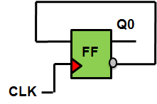
    Since the LSB i.e. Q0 toggles itself at every clock cycle, the 1-bit Johnson Counter can be used for Q0. Note that here we are using bit-by-bit synthesis instead of the conventional Karnaugh map approach to design our binary counter.

  • Similarly, higher order counter bits can be realized by higher order Johnson Counter, where the last bit would represent the binary counter bit. For Q1, the circuit would be:
  • The same can be extended in a recursive manner to design any n-bit binary counter.
  • Note that in this design, there is absolutely no combinatorial cells between any two registers, thereby making high operating speed possible.

    Time Period of the Clock ≥ T(clk-to-qbar),FF + Tsu,FF

    What is the trade-off here? The answer is dynamic power dissipation. Note that a conventional n-bit counter would use n flops. However, for the proposed design, 3-bit counter would need (1+2+4=) 7 flops, 4 bit counter would need (1+2+4+8=) 15 flops and so on. This design might find practical application for lower order counter widths like 4-6. 

    Above that, the design would dissipate too much power to be of any practical use.

July 12, 2013

Placement of Clock Gating Cells

Clock Gating Cells are indispensable components to save dynamic power. However, the backend design engineers must be prudent while placing them. In this post, I'll talk about the trade-off between timing and power that underlies the placement of clock gating cells.

Consider that your SoC has two IPs, and a single clock source. These two IPs are synchronous, and might work independently (i.e. without any interaction with the other IP) in some use-case of the chip. This entails the need of two clock gating cells. Now the question arises: where to place these clock gating cells. 
  • Near the sink, i.e. the clock source, or
  • Near the source, i.e. the respective IPs
Let's take up pros and cons of the two placement scenarios.


  1. Clock Gating Cells placed near the source: As shown in the figure, placing the clock gating cells near the clock source, can  the increase the uncommon clock path (shown in yellow). 


Recall from the post: Common Path Pessimism that while doing timing analysis, the effect of OCV derates come into picture for the uncommon clock path because the clock tree buffers in the uncommon path can behave differently and hence an STA engineer needs to take into account that extra uncertainty or pessimism while doing timing analysis. Such a scenario is therefore hostile to the timing engineers. However, from power perspective this scheme is quite favorable. Since as soon as the clock gate is turned "Off", all the clock buffers in the fanout of that clock gate are also "off" or in other words, they do not toggle and hence do not dissipate dynamic power. Like any engineering problem, there exists a trade-off between two conflicting factors, and designers often need to prioritize.

2. Clock Gating Cells placed near the sink: While this scenario, with greater common path as compared to the first scenario and hence making the timing easier to met, is not friendly from the power perspective. 
All the clock tree buffers  in the common clock path (shown tin red) lie before the clock gate and hence would always be "on" and keep on toggling at the clock frequency, thereby dissipating dynamic power.


Solution:
The pertinence of a solution is dictated on many factors. Permissible clock latencies, power dissipation specifications, timing closure challenges and also the use-case.

Let's say we had a requirement that IP 2 will function if and only if IP 1 is on. In this case we could have placed the clock gates in series like this:


By having the two clock gates in series, we would save the dynamic power of all the clock tree buffers in the fanout of first clock gate. Moreover, the uncommon path is significantly less as compared to the scenario 1.

Again note that this solution would not work if we had the use-case where IP 1 could be "off", while IP 2 still "on".