August 15, 2013

Integrated Clock and Power Gating

Clock Gating and Power Gating are two most commonly used design methods to save dynamic and leakage power respectively. How about integrating the two solutions such that they complement each other? In this post, I will talk about a simple way to do so.

Clock Gating is accomplished by using Clock Gating Integrated Cell (CGIC) which gates the clock to the sequential elements present in its fan-out when the enable signal is logic 0. Power Gating structures may be of two types: Simple Power Gating and State Retention Power Gating. Using the former technique, the output of the logic gates slowly leaks the charge at the output and thereby when the SLEEP signal is de-asserted, one cannot predict the logic value at the output. The latter technique is able to retain the state at the output which was last present before asserting the SLEEP signal.

Let's take up a few plausible scenarios:
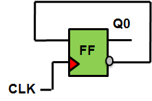
  • Case I - Normal Case: Which employs  only conventional clock gating. It is depicted in the figure.
 

  • Case II - When one does not need to retain the states of the combinatorial cells or the sequential elements. One possible scenario could be in the case of a standalone IP, which is not comunicating with any other IP on the SoC. Here one can use thee simple power gating where the SLEEP signal is derived from the CGIC itself using a latch, as depicted in the figure below. Doing so, we would save both dynamic and leakage powers. 


  • Case IIII - When one does not need to retain the states of the combinatorial cells, but the sequential outputs need to be safe-stated. Possible use-case could be where only the sequential outputs communicate with other IPs on the SoC. This can be accomplished by using State Retention Flip Flops instead of the conventional flip-flops.
  • Case IV - When both the combinatorial cells and the sequential cells interact with other IPs. But the previous value need not be required. Since it is a classic case of interaction between "switchable power domain" with" always ON", it entails the use of isolation cells between such power domain crossings. It must be noted that in such a case, isolation cell would always be present in the always  ON power domain, i.e., it would receive it's VDD supply from the always ON power domain supply. This is because, when the switchable power domain in OFF, the isolation cell can function only if receives the power supply! 
Isolation Cells can be simple cells like AND or an OR gate, which receive one input in a way that, irrespective of the second input coming from the switchable power domain, the value would be controllable. For example, logic 0 for AND gate and logic 1 for an OR gate. I will try to take this up in a separate post.

July 20, 2013

High Speed Counter Design

In this post, I'll talk about the limitations associated with the conventional binary counter design in terms of it's maximum operating frequency, and also discuss an ingenious yet simple design (not invented by me!) which can operate at a very high frequency.

Conventional Binary Counter: The operating speed of any binary counter, or for that matter, any sequential circuit is governed by the setup time limitation that the combinatorial logic between any two registers (flip-flops). Note that:
  • Any higher-order counter bit toggles only when all the lower-order bits are logic 1.
  • The input for any higher-order counter bit is a function of all the lower-order bits and itself during the last clock cycle.
  • The operating speed for an n-bit counter is limited by the following equation:

    Time Period of the Clock
    T(clk-to-q),FF0 + (n-2).TAND + TXOR + Tsu,FF(n-1)
     
  • The following figure shows the circuit for a 4-bit conventional binary counter. It must be noted as as the counter width increases, the operating frequency decreases.

High Speed Binary Counter: How about designing a binary counter where there is no combinatorial cells between any two registers, so that such a design is able to achieve the highest operating frequency for a given technology node? For this counter the basic premise is:
  • Since the counting sequence for any counter bit is deterministic in nature, it should be possible to design a counter in a manner that: each bit is a function of only itself over all the previous clock cycles.
  • Johnson Counter enables us to design in such a manner that there is no combinatorial cell between any two registers. Let's have a look:
    Since the LSB i.e. Q0 toggles itself at every clock cycle, the 1-bit Johnson Counter can be used for Q0. Note that here we are using bit-by-bit synthesis instead of the conventional Karnaugh map approach to design our binary counter.

  • Similarly, higher order counter bits can be realized by higher order Johnson Counter, where the last bit would represent the binary counter bit. For Q1, the circuit would be:
  • The same can be extended in a recursive manner to design any n-bit binary counter.
  • Note that in this design, there is absolutely no combinatorial cells between any two registers, thereby making high operating speed possible.

    Time Period of the Clock T(clk-to-qbar),FF + Tsu,FF

    What is the trade-off here? The answer is dynamic power dissipation. Note that a conventional n-bit counter would use n flops. However, for the proposed design, 3-bit counter would need (1+2+4=) 7 flops, 4 bit counter would need (1+2+4+8=) 15 flops and so on. This design might find practical application for lower order counter widths like 4-6. 

    Above that, the design would dissipate too much power to be of any practical use.

July 12, 2013

Placement of Clock Gating Cells

Clock Gating Cells are indispensable components to save dynamic power. However, the backend design engineers must be prudent while placing them. In this post, I'll talk about the trade-off between timing and power that underlies the placement of clock gating cells.

Consider that your SoC has two IPs, and a single clock source. These two IPs are synchronous, and might work independently (i.e. without any interaction with the other IP) in some use-case of the chip. This entails the need of two clock gating cells. Now the question arises: where to place these clock gating cells. 
  • Near the sink, i.e. the clock source, or
  • Near the source, i.e. the respective IPs
Let's take up pros and cons of the two placement scenarios.


  1. Clock Gating Cells placed near the source: As shown in the figure, placing the clock gating cells near the clock source, can  the increase the uncommon clock path (shown in yellow). 


Recall from the post: Common Path Pessimism that while doing timing analysis, the effect of OCV derates come into picture for the uncommon clock path because the clock tree buffers in the uncommon path can behave differently and hence an STA engineer needs to take into account that extra uncertainty or pessimism while doing timing analysis. Such a scenario is therefore hostile to the timing engineers. However, from power perspective this scheme is quite favorable. Since as soon as the clock gate is turned "Off", all the clock buffers in the fanout of that clock gate are also "off" or in other words, they do not toggle and hence do not dissipate dynamic power. Like any engineering problem, there exists a trade-off between two conflicting factors, and designers often need to prioritize.

2. Clock Gating Cells placed near the sink: While this scenario, with greater common path as compared to the first scenario and hence making the timing easier to met, is not friendly from the power perspective. 
All the clock tree buffers  in the common clock path (shown tin red) lie before the clock gate and hence would always be "on" and keep on toggling at the clock frequency, thereby dissipating dynamic power.


Solution:
The pertinence of a solution is dictated on many factors. Permissible clock latencies, power dissipation specifications, timing closure challenges and also the use-case.

Let's say we had a requirement that IP 2 will function if and only if IP 1 is on. In this case we could have placed the clock gates in series like this:


By having the two clock gates in series, we would save the dynamic power of all the clock tree buffers in the fanout of first clock gate. Moreover, the uncommon path is significantly less as compared to the scenario 1.

Again note that this solution would not work if we had the use-case where IP 1 could be "off", while IP 2 still "on".

June 09, 2013

Reversible Logic Gates

Who would have thought that even digital logic gates could be reversible in nature? Well, as it turns out, there's been a lot of research already done on the subject. In this post, I would only discuss the motivation behind building reversible logic gates.

Every node can be generalized as a capacitance that would undergo charging/discharging depending upon the inputs and the logic that that particular gate has been designed to realize. And every node would dissipate charge in form of leakage power. What if someone takes the output and feeds it back to the inputs forming a "Positive Feedback" structure! In order words, one can sustain the inputs from outputs and outputs would anyway be dependent on inputs. Doing so can save a lot of leakage power and this exactly is the motivation behind building reversible logic gates. Cool, isn't it? Have a look below where C is any combinatorial logic gate.

It might be easier to appreciate the advantage of such a logic gate when many of them are attached in cascade as shown below. Here the output of one gate would sustain it's input which, in turn, would be the output of some other logic gate and it would continue on forever!! 


Enough said. Here's the paper: Efficient Building Blocks for Reversible Sequential Circuit Design by Hari, Shroff, Mahammad & Kamakoti which you can read to understand the implementation better. Please let me know in case you come across any work related to "Reversible Logic Gates".


June 08, 2013

Dual-Edge Triggered Flip Flop

Dual-edge triggered flip-flop is a sequential element which samples data at both positive as well as negative edges of the clock. This might come in handy in applications where the throughput is very high. It might come as a surprise that modern standard cell libraries do not have a dual edge triggered flop! Therefore, that leaves the designer to make a dual-edge triggered flop using the available standard cells. Over the years, many such designs have been proposed. While, they all work, in this post, we would discuss their pros and cons from the perspective of design, timing and power dissipation.

Implementation #1

The only possible cons with this circuit are:
  • STA would need to meet the clock gating checks at the both inputs of the multiplexer.
  • And here, the clock is used as a data which is a scenario that one would ideally like to prevent in their designs. 
  • The multiplexer would dissipate a considerable dynamic power because it's one input would be toggling at quite a high frequency.

Implementation #2
Psuedo-Dual Edge Triggered Flip Flop by Ralf Hilderbrandt 
 The possible concerns with this circuit could be:
  • The setup time and clk-to-q delay of the "dual" edge triggered flip flop would be:

    Total Setup Time = Setup time of single Flop + delay of a XOR Gate
    Clk-to-q delay      = Clk-to-q delay of a single flop + delay of a XOR Gate

    This can be quite a large value and therefore will reduce the time available for the data combinatorial logic between any two flip-flops.
  • Secondly, as the input at D would toggle (before eventually getting stable setup-time before the clock edge), and hence the XOR gates would toggle. XOR gates being the most bulky of all the primitive logic gates, the dynamic power dissipation of this flop would be quite high!

It is therefore important to discern which flop might be suitable for you. One might also look to make changes as the transistor level to achieve a better performance dual edge-triggered flip-flop. Please drop me a mail along with the weblink for such a paper in case you come across one.


June 02, 2013

Faulty Clock Gating: How "Not" to Gate the Clock

You would come across a plethora of technical literature on clock gating and it's associated techniques. It does not come as a surprise because clock gating is the most commonly employed design technique to save dynamic power. However, many implementations are faulty, in the sense that while they indeed gate the clock, but the result in an overall increased dynamic power consumption. We would discuss one such common technique, which obviates all the power saving benefits of clock gating. You are advised to use your discretion before using it.

The basic rationale behind clock gating:
  • Even when the output of a flip-flop is not toggling, owing to the transitions (and hence charging/discharging of nodes) in the internal circuitry of the flop-flop, it still continues to dissipate dynamic power when it is being fed by a clock signal.
  • When the input of the flip-flop is not toggling or would not toggle, one can effectively gate the clock to that flip-flop for that particular time and save dynamic power. 
One logical implementation for the above problem statement (and this is indeed the implementation employed in many technical papers and patents) is depicted below:


Let's take a look at the above implementation. The XOR gate between the D input and the Q output of the flip-flop has been used as the enable signal for the clock gate CGIC. The logical explanation behind this is: when the output of the flop is same as input, which would be detected by XOR'ing the two, one can gate the clock to the clock gate.
Example: Let's say initially Q =1. Now D = 1, which means that t he output of the flop is destined to stay at "1" for the next cycle as well. XOR'ing these two signals: Q XOR D = 0, EN = 0 would gate the clock to the flip-flop. So, would that save power? Well, one would expect it that way. Let's take a look at why it would result in an increased power dissipation.

The circuit shown above is a trap! The actual circuit would be something like the one shown below:

  • As evident from the above figure, the  XOR gate would continue to toggle for the entire time period of the clock and would become stable only "setup time" before the next clock edge. And during this entire duration, it would continue dissipating dynamic power. You might argue here that the power dissipated must be less than the power dissipated by an idle flop receiving clock. Well, that might be true for some technology, but XOR gate is the most bulky gate (among all primitive gates) and I would say that this power, if not less, would at least be comparable to that of an idle flop receiving a clock signal.
  • Secondly, the circuit above uses a CGIC. Note that CGIC comprises off one latch and an AND gate, while a flop comprises  of two latches. The internal circuitry of the CGIC would continue to charge/discharge and hence dissipate power.
The sum of the above two power dissipation would over-shadow the benefits one was expecting in the first place, and hence it  is a common design trap. Beware of it.


May 15, 2013

Common Path Pessimism

Common Path Pessimism is a common source of some extra pessimism in timing analysis. Before we delve further into this, note that pessimism can be of two types: Intended and Unwanted. Intended pessimism could be like adding some extra uncertainty for clock skew before CTS stage, or some uncertainty for noise before SI (Signal Integrity) analysis. It is often prudent to have this pessimism taken upfront in your design because it will avoid any surprises when you move from one stage to another. 

Having said that, which category do you reckon should Common Path Pessimism fall? Let's define it first and then we'll take a look at it objectively.

When any pair of launching and capturing flop have a some portion of clock path as common, the difference between the max and min delay of that common clock segment is referred to as Common Path Pessimism. We discussed the rationale behind the use of timing derates briefly in the post: OCV vs PVT. Note that the entire timing analysis revolves around this intended pessimism where the basic aim is to make the timing paths more critical to avoid seeing any surprises in the silicon. EDA tools, however, themselves have quite a fair amount of pessimism, it is always prudent for the STA engineers to augment some uncertainty/pessimism in their timing analysis.

Convince yourself that:
  • Setup check would be most critical when clock reaches the launching flop late and capturing flop early; and the data path takes more delay.
  • Hold check would be most critical when clock reaches the launching flop early, capturing flop late and data path takes less delay.
Consider the following example with no common clock path and note that we have just applied the above principle to add pessimism in timing analysis.


So, while doing setup analysis, the clock tree buffers in the launching path would be derated by +5% and in the capturing path would be derated by -5&. The data path would be derated by +5%.
While doing hold analysis, it would be the opposite. The clock tree buffers in the launching path would be derated by -5% and in the capturing path would be derated by +5&. The data path would be derated by -5%.

How would the situation change when there's a common clock path? Let's take a look.
Ideally speaking, for setup analysis, we would like to take the +5% derated value of the delay of these buffers while considering launching path and -5% derated value while considering the capture path. However, here lies the catch! How can the same buffer or set of buffers be derated differently for launch and capture? Recall from the definition of OCV that it is the intra-chip variation in PVT that STA engineers consider them in the first place.

However, now these buffers, they are in the same location. So at a time they would behave in a similar manner. It does not make sense to consider different delays for same buffers. And this is the origin of common path pessimism and in usually unwanted. What we can do is (or rather what EDA tools tend to do is), do the calculation considering common path to be non-existent. And in the slack, add the double derated value of the common buffers, which would be 10% of the three common buffers in this case. This is referred to as Common Path Pessimism Removal.

May 04, 2013

Combinational Loops

You would often hear backend engineers remonstrating the frontend design folks on the presence of combinational loops in the design. But why do they create such a hue and cry? What possibly could one or maybe few combinational loops do? Well, potentially, they can render the entire functionality of the SoC haywire and not taken care off. And some combinational loops, on the other hand, are indispensable for the evolution of a particular technology. We'll see how and why.

A combo loop is structure which is formed by a signal starting from an input of a combinational gate, after passing through one or more combinational gate, reaches the same combo gate from which it started without encountering any sequential element in between.

Here's what a generalized combo loop looks like:


  • Unstable Loops: Let's start with a basic combo loop that you must have studied in your academics or at least heard about it. The reverend Ring Oscillator. It is an inveterate fallacy that a ring oscillator can be used to make a clock generating circuit. Trust me, clock generating or even divider circuits, for that matter, are not as simple as the ring oscillator shown below. 


Of what use could this simple circuit be? Well, if we can control any one input of any of the three inverters shown here, we can know the delay of an inverter which is often the first cell to be characterized in any technology. Moreover, test structures like these also help the foundry guys in determining the manufacturing process of a particular chip whether it was WCS or BCS.
  • Stable Loops: Here's an example of a stable loop consisting of an OR gate. Note that, as soon as the free input receives a logic 1, the output goes to 1. And same signal is conveyed back to the another input, and the loop is stable or rather stuck-at-1.

Note that stable loops would not pose problems of copious dynamic power consumption. But such a loops pose headaches to DFT teams. Recall from the post: Two Pillars of DFT: Controllability & Observability, we talked about how stuck-at faults are simulated and detected. If such a loop would be present in the design, any stuck-at faults in the vicinity of this gate cannot be observed, and hence DFT team would lose their stuck-at coverage by a considerable amount!!

STA Concerns: We started this post with a preamble talking about backend engineers repining the frontend engineers. How would a backend engineer be affected by a combo loop? Here's how.

Recall from the post: Factors Affecting Delays of Standard Cells that the delay and output slew of any standard cell depends on the input slew and output load. The below figure shows one such example, where slew can keep on degrading indefinitely, and would ultimately impact the timing and more importantly the power consumption of the SoC.

To sum up, combo loops must be avoided in all SoCs except for special circumstances like ring oscillator circuit can be employed for testing the characteristics of the SoC.


April 21, 2013

Puzzle: DFT Shift Frequency

It is a well known fact that DFT Shifting is done at a slower frequency. Well, I'm gonna list down some cons against this. You'll have to tell the pros!

  • Lower is the frequency, greater is the test time. In modern SoCs, tester cost  (which is directly proportional to the tester time) accounts for roughly 40% of the selling price of a single chip. It would be pragmatic to decrease the test time by increasing the frequency. No?
  • Increasing the frequency would not pose any timing issue. Because, hold would anyway be met (Hold check is independent of frequency). And setup would never be in the critical path considering the fact that scan chains only involve direct path from output of a flop to scan input pin of the next flop, devoid of any logic.

Then why not test at a higher frequency, which is at least closer to the functional frequency? What could possibly be the reason for testing at slower frequency?

April 19, 2013

Puzzle: Stuck-At Fault

A brief introduction to Stuck-At Faults was given in the post: Design for Testability: Need for Modern VLSI Design. You might want to go through it first. Anyway, as the name suggests, stuck-at faults manifest themselves if any particular node  in the design is "stuck" at either 0 or 1. A plausible explanation for stuck-at-0 (SA0) might be that the particuular node on question has somehow been shorted to Ground (GND at 0V) . Similarly, a node might be Stuck-At-1 (SA1) if let's say it is somehow shorted to the VDD (at logic 1).

In order to detect a stuck-at-0 fault, we would try to excite that node to the opposite value, i.e. 1 and try and see if we are able to achieve that. If we are able to do so, we can safely say that the node in question in NOT stuck-at-0. And vice-versa.

In the below question, we intend to check the node X for a stuck-at-0 fault. Can you tell what input vector (A,B,C) would be need to give to do so?


Two Pillars of DFT: Controllability & Observability

I haven't given an equitable share of attention to DFT, and now, it's time to make some amends! Just like Timing is built on two pillars: Setup & Hold, entire DFT is built on two pillars: Controllability & Observablity.  Very often you would find DFT folks cribbing that they can't control a particular node, or don't have any mechanism to observe a particular node in question. You may like to review the previous post: DFT Modes: Perspective before proceeding further.

Shifting our attention to the pillars of DFT, let's define the two.
  • Controllability: It is the ability to have a desired value (which would be one out of 0 or 1) at any particular node of the design. If the DFT folks have that ability, they say that that particular node is 'controllable'. Which in turn means that they can force a value of either 0 or 1, on that node!
  • Observability: It is the ability to actually observe the value at a particular node whether it is 0 or 1 by forcing some pre-defined inputs. Note that, unlike the circuit that we make on paper, the SoC is a colossal design and one can observe a node only via the output ports. So, DFT folks actually need a mechanism to excite a node and then fish that value out of the SoC via some output port and then 'observe' it!
Ideally, it is desired to have each and every node of the design controllable and observable. But reality continues to ruin the life of DFT folks! (Source: Calvin & Hobbes). It is not always possible or rather practical to have all the nodes in a design under your control, because of the sheer complexity that modern SoCs possess. And therefore, it is the reason you would hear them talk about 'Coverage'. Let's say coverage is 99%, this means that we have the ability to control and observe 99% of the nodes in the design (A pretty big number, indeed!).

Now let's take some simple examples.
In the above example, if we have control the flops such that the combo cloud results in 1 at both the inputs of AND gate, we say that the node X is controllable for 1. Similarly, if we can control any input of AND gate for 0, we say that node X is controllable for 0. Similarly, let's say we wish to observe the output of FF1. If we can somehow replicate the value of FF1 by making the combo clouds and AND gate transparent to the value at FF1, we say that output of FF1 is observable. Intuition tells us that for AND gate to be transparent, we should have the controllability of other node for 1. Because when one input of AND gate is 1, whatever is the value at the other input, it is simply passed on!!

April 17, 2013

Low Power Synthesis: Insertion of Clock Gating Cells

Power consumption is a growing concern for modern SoCs and design engineers today face an arduous task of limiting the power dissipation of their SoCs. It would be unfair to think the backend design cycle as a magical solution to all the power solutions. However, modern synthesis EDA tools are smart enough in identifying some key RTL constructs and synthesizing a low power equivalent of the structure. We will take a look at one such RTL Construct and it's equivalent implementation for low power design.

Consider the following behavioral description:

always @ ( posedge clk )
begin
   if (enable == 1'b1) then
   q [15:0] <= d [15:0]
end

One logical implementation and the corresponding low power implementation of the above description would be:

The synthesis tools find such RTL constructs and try and convert it into the low power implementation shown above. Please note that, the clock gating integrated cell (CGIC) also consumes power and the above implementation might not be an expedient solution if the above enable is mostly high, or even if the number of registers in the register set is small. Therefore, one needs to exercise caution while using or implementing such a structure!

April 13, 2013

Clock Jargon: Important Terms

Clock to an SoC is like blood to a human body. Just the way blood flows to each and every part of the body and regulates metabolism, clock reaches each and every sequential device and controls the digital events inside the SoC. There are many terms which modern designers use in relation to the clock and while building the Clock Tree, the backend team carefully monitors these. Let's have a look at them.

  • Clock Latency: Clock Latency is the general term for the delay that the clock signal takes between any two points. It can be from source (PLL) to the sink pin (Clock Pin) of registers or between any two intermediate points. Note that it is a general term and you need to know the context before making any guess about what is exactly meant when someone mentions clock latency.
  • Source Insertion Delay: This refers to the clock delay from the clock origin point, which could be the PLL or maybe the IRC (Internal Reference Clock) to the clock definition point.
  • Network Insertion Delay: This refers to the clock delay from the clock definition point to the sink pin of the registers.
Consider a hierarchical design where we have multiple people working on multiple partitions or the sub-modules. So, the tool would be oblivious about the "top" or any logic outside the block. The block owner would define a clock at the port of the block (as shown below). And carry out the physical design activities. He would only see the Network Insertion Delay and can only model the Source Insertion Delay for the block.

Having discusses the latency, we have now focus our attention to another important clock parameter: The Skew.

We discusses the concept of skew and it's implication on timing in the post: Clock Skew: Implication on Timing. It would be prudent to go through that post before proceeding further. We shall now take the meaning of terms: Global Skew and Local Skew.
  • Local Skew is the skew between any two related flops. By related we mean that the flops exist in the fan-in or fan-out cone of each other.
  • Global Skew is the skew between any two non-related flops in the design. By non-related we mean that the two flops do not exist in the fan-out or fan-in cone of each other and hence are in a way mutually exclusive.
In the next post we would discuss the implications of big clock latency on the timing. Please feel free to post your thoughts at my<dot>personal<dot>log<at>gmail<dot>com.

March 17, 2013

Puzzles: Half Adder using Multiplexer

Let's say you have to realize a half adder. But all you've got are 2:1 Multiplexers. How would you design one half adder using ONLY 2:1 Multiplexers?

Click here to find the solution:

Low Power FSMs

Low Power design is the need of the hour! The post: Need for Low-Power Design Methodology gives an insight into the intent and need for the modern design to be power aware. The subsequent posts on Clock Gating and Power Gating under the tab Low Power Methodology discuss some ways in which the the SoC can be designed for low power. In this post, we will consider one such low power design of an FSM which can be generalized to design any low power sequential circuit.

Consider the following generalized design of a traditional and a low power FSM:

Let's talk about the basic building block that we have used here. The OR gate acts as an clock gate to the flop. The flop that we have used is a toggle flop. When enable = 0, the flop receives the clock, and the flop toggles its state. So, whenever we need to change the state of the flop, we can give a clock pulse.

Enough said! Let's now talk about a real example of a basic synchronous counter. And how we can design a low power synchronous counter using the above method.

In any binary counter:

  • The lowest order bit toggles after every clock cycle.
  • Any higher order bit toggles only when all the lower order bits are at logic 1.
Keeping this in mind, we can now build the low power counter!!

March 14, 2013

VLSI-SoC: Now on Facebook!!


Hey guys! Check out our new Facebook page and stay connected to all the latest posts and puzzles! Just "like" the page and find all the latest updates right on your wall!

You can find our Facebook page at the below link:

VLSI-SoC Facebook Link

Please help us reach out your friends and colleagues. Thanks in advance for your support!!


March 12, 2013

Multi-Cycle Paths: Perspective & Intent

Multi-Cycle Paths, as the name suggests, are those paths which need not be timed in one clock cycle. It is easier said than done! Before we discuss further, let's talk about what Multi-cycle paths does not mean!!

Myth 1: All those paths which the STA team is unable to meet at the highest clock frequency, are potential multi-cycle paths.
Reality: Multi-cycle paths are driven by the architectural and design requirements. STA folks merely implement or appropriately said, model the intent in their timing tools! A path can be a multi-cycle path even if the STA team is able to meet timing at the highest clock frequency.

Myth 2: It is by some magic that the design teams conjure up how many cycles it would be appropriate to for a path to function! <Apologies the hyperbole! :)>. And STA team follows the same in their constraints.
Reality: MCPs are driven by the intent. And implementation is governed by that intent which includes but is not limited to the number of run modes a particular SoC should support.

Consider the following scenario:

Normal mode, Low Power Mode and Ultra Low Power Modes can be considered to be the different run modes of the SoC. You can say that the customer can choose at what time which run mode would be better. Example: when performance is not critical, or your device can go to 'hibernate' mode, you (or the software) can allow the non-critical parts of the SoC to go into a Low Power Mode, and hence save power!

Consider the specifications:
  • Normal Mode: Most Critical IP & Not-So Critical IP would work at f MHz. Least Critical IP would work at f/2 MHz. Interaction between any two IPs would be at slower frequency.
  • Low Power ModeMost Critical IP would work at f MHz. Not-So Critical IPLeast Critical IP would work at f/2 MHz. Interaction between any two IPs would be at slower frequency.
  • Ultra Low Power ModeMost Critical IP would work at f MHz. Not-So Critical IP would work at f/2 MHz. And Least Critical IP would work at f/k MHz; (k=> 3-8). Interaction between any two IPs would be at slower frequency.
Consider the Low Power Mode. Any interaction within the Not-So Critical IP would be at slower frequency. However, any paths between the Most Critical IP and Not-So Critical IP would be Multicycle path of 2 in the low power mode. In this case, the clock at the Not-So Critical IP is gated selectively for every alternate clock cycle to implement an MCP. Hence data launched from Most Critical IP now effectively gets two clock cycles (of the faster clock) to reach the Not-So Critical IP. The following figure explains the intent:


This much for the intent! However, as we mentioned that for the Least Critical IP, depending on the mode, would work at f/k MHz => (k=3-8) one might need an MCP of 2, 3, 4.... and so on. This calls for a need of a configurable implementation of multicycle paths. We shall cover it sometime later. Till then, you can assimilate on the intent part. You can also mail me in case you think of any such implementation at my<dot>personal<dot>log<at>gmail<dot>com. Adios!

State Retention Power Gating

The post titled Power Gating demonstrated the implementation of a Power Gating Cell and how it helps in minimizing the leakage power consumption of an SoC. Make sure you go through it once more. The basic rationale is to cut the direct path from the battery (VDD) to ground (GND). Though efficient in saving the leakage power, the implementation discussed suffers from one major drawback! It does not retain the state! That means, once power of the SoC is restored, the output of the power gated cell goes to 'X'. You can't really be sure whether it is logic 1 or a logic 0. Do care? Yes! Because if this X propagates into the design, the entire device can go into a metastable state! In order to prevent such a disastrous situation: the system software can simply reset the SoC. That would boot-up from scratch and make sure that all the devices are initialized. 

This means, every time I decide to power gate a portion of my SoC, I'll have to reset that power gated portion once power is returned. This imposes a serious limitation to the application of the Power Gate discussed in the last post. How about designing one power gate which retains the state? But convince yourself that in order to do so, you'd need to spend, though small, some leakage power. Let's call this structure: State Retention Pseudo Power Gate. The term "pseudo" signifies that it would consume a little leakage power contrary to the previous structure which doesn't. But at the same time, you no longer need to reset the power gated portion of the SoC, because the standard cells retain their previous data!! Enough said! Let's discuss the implementation.

The above circuit has two parts. 
  • The one inside the red oval is same as the normal power gating structure. 
  • The one inside green box (on the right) is the additional circuitry required to enable this device to retain it's state.
Operation: Let's say before going into the SLEEP mode, the device had the output as logic 1. After entering the SLEEP mode (power off), the sleep transistors come into action and cut the power and ground rails of the device and hence save the leakage power. But the logic on the right (in green rectangle) is still ON! The output of the inverter would now become OUTPUT', i.e., logic 0. This would in turn enable the PMOS transistor Q1 and output would be restored back to logic 1.
Same is true when the output would be logic 0 before power gating. In that case the NMOS transistor Q0 would come into action to help the output node retain it's data.

Note that: All this while, when the device is in sleep mode, the output node would continue to leak. By adding the additional circuitry, as demonstrated, we are basically trying to create a feedback loop, which again helps in retaining the state. The hit, of course, is the leakage power of 4 transistors. However, the standard cell logic (in red oval) is usually bulky. Even a simple 2-input NAND gate has 4 transistors itself. And higher order input would have more! Same technique can be applied to any sequential device like a Flip Flop, latch or even a clock gating integrated cell.

March 09, 2013

Post Your Queries

Hello friends. It's been 9 months since we started writing. And we have crossed 12K page views since then. I would like to take this opportunity to thank each and every one of you for their precious comments. It really does motivate me to keep writing more! Also, it gives me immense pleasure to know that there are people out there who are reaping benefits out of it! I know we have a long way to go and to do so, I would be grateful if I can hear your feedbacks and suggestions regarding the same. 

Please note that I have made some changes to the blog settings. 
  • Unlike before, one would require to log-in using their Google accounts to comment on the blog. I hope you would appreciate the necessity behind it.
  • I have updated another page: 'Post Your Query' to enable readers to post their own doubts, and if you wish me to cover any specific topic, you can also mail me at my<dot>personal<dot>log<at>gmail<dot>com
  • This is only on a trial basis. Let's see how it all shapes up!

OCV vs PVT

In the post PVTs and How They Impact Timing, we talked about the confluence of the Process-Voltage and Temperature factors and their impact on timing. I would urge the readers to go through the post in order to grasp the difference between two key terminologies used in the VLSI industry- 

  • OCV: On Chip Variation;
  • PVT: Process, Voltage and Temperature
While PVTs are inter-chip variation which depend largely on external factors like: the ambient temperature; the supply voltage and the process of that particular chip at the time of manufacturing. Like PVTs, OCVs are also variations in process, voltage and temperature. But, hey, where's the difference? OCVs are intra-chip variations! To elucidate more about the OCVs, let's talk in terms of chips!

  • Variation in Process: There are millions of devices (standard cells); and probably billions of transistors packed on the same chip. You can expect every single transistor to have the same process or the channel length! If we say that the chip manufactured exhibits, let's say, worst process, it means that the  channel length tends to deviate towards the higher side. This variation may be more for some transistors and less for some. It can be a ponderous task to quantify this variation between the transistors of the device, and is often modeled as a percentage deviation from the normal.
  • Variation in Voltage: All the standard cells need voltage supply for their operation. And voltage is usually 'tapped' from the voltage rail via interconnects which have a finite resistance. 


In two parts of the chip, it is fairly probable for the interconnect length to be different, resulting in a finite difference in the resistance values and hence the voltage that the standard cells actually receive. As evident above, the voltage received by the standard cells on the right would be less as compared to those on the left.

This variation would be less, probably of the order of a few mili-volts, but is can be significant, is again modeled as OCV.
  • Variation in Temperature: Some parts of the chip can be more densely packed or might exhibit more active switching ss compared to the other parts. In these regions, there is a high probability of the formation of localized 'HOT SPOTS' which would result in increased temperature in some localized areas of the chip. Again, this difference might be order of a few degree centigrade, but can be significant.
All the above mentioned variations are examples of On-Chip-Variations. And usually, these variations are modeled as a fixed percentage of delays. For examples, a 4% OCV derate would mean, that the delays of cells in the data path are inflated by 4% while doing setup analysis and decreased by 4% while doing hold analysis. Same methodology is applied for the clock paths. However, it would be different for launching and capture clock paths. That also gives rise to an interesting topic of Common Path Pessimism Removal which we shall take up shortly. 

Clock Skew: Implication on Timing

Clock Skew is an important parameter that greatly influences the timing checks and you would often find the backend design engineers always keeping a close eye on the clock skew numbers. 

Clock Skew: The difference in arrival times of the clock signal at any two flops which are interacting with one another is referred to as clock skew. Having said that, please note that skew only makes sense for two flops which are interacting with one another, i.e. they make a launch-capture pair. 
If the clock at the capture flop takes more time to reach as compared to the clock at the launch flop, we refer to it as Positive Clock Skew. And when the clock at capture flop takes less time to reach the clock at the launch flop, we refer to it as Negative Clock Skew.
The figure below describes positive & negative clock skew. Assume the delays of clock tree buffers to be the same.
How does clock skew impact the timing checks, in particular, setup and hold? Consider the above example where FF1 is the launching flop and FF2 is the capturing flop. If the clock skew between FF1 and FF2 was zero, the setup and hold checks would be as follows:

  • Positive Skew: Now imagine the case where clock skew is positive. Here, clock at FF2 takes more time to reach as compared to the time taken by the clock to reach the FF1. Recall that the setup check means that the data launched should reach the capture flop at most setup time before the next clock edge. As evident in the below the data launched from FF1 gets an extra time equal to the skew to reach FF2. Hence setup is relaxed! However, hold check means that data launched should reach the capture flop at least hold time after the clock edge. Hence, the hold is further made critical in case of positive skew. Read the definitions again and again till you grasp it!!

  • Negative Skew: Here, clock at FF1 takes more time to reach as compared to the time taken by the clock to reach the FF2. As evident in the below the data launched from FF1 gets lesser time equal to the skew to reach FF2. Hence setup is more critical! However, hold is relaxed!
    Some Key Points to Note:
  • Setup is the next cycle check, and positive skew relaxes the setup check and negative skew further tightens it.
  • Hold is the same cycle check, and negative skew relaxes the hold check and positive skew further tightens it.
  • Very rarely would one come across a path that is both setup as well as hold critical. Setup becomes critical when data path is huge or you have a large negative skew; and hold becomes critical when either data path is minimal or you have a large positive skew. Both these conditions are mutually exclusive and very rarely does they manifest themselves simultaneously. It is often a case when the uncommon clock path is significant. We shall discuss it in detail later.

February 09, 2013

Puzzle: CMOS

Let's say you have a 2-input CMOS NAND Gate. Due to some design pre-requisite, it is always ensured that the input A goes from low-to-high before the input B. 


In order to optimize the delay of the NAND Gate, which on out of the 2 configurations would you choose and why?


February 08, 2013

Puzzle: Fixing Timing Violation

Timing Violation can manifest due to a plethora of reasons. And it is important for an STA Engineer to understand the violating path and model the constraints properly before providing them to the Synthesis/PnR tools for optimization. Unnecessary optimization should be avoided because:
  • To save on the die area;
  • To save on the leakage power;
  • To prevent unnecessary congestion.
The figure below shows a scenario. Assume the clock period to be 8ns and the setup time of the capture flop (here, FF3) be 0ns and the clock-to-Q delay of the launch flops (here, FF1 & FF2) be 0ns. The violating path is shown in the figure. The negative slack is 1ns. 


How would you fix the above violation? Please note that there are many possible solutions; but one only solution adheres to the above discussed constraints of leakage power, area and congestion.