July 20, 2013

High Speed Counter Design

In this post, I'll talk about the limitations associated with the conventional binary counter design in terms of it's maximum operating frequency, and also discuss an ingenious yet simple design (not invented by me!) which can operate at a very high frequency.

Conventional Binary Counter: The operating speed of any binary counter, or for that matter, any sequential circuit is governed by the setup time limitation that the combinatorial logic between any two registers (flip-flops). Note that:
  • Any higher-order counter bit toggles only when all the lower-order bits are logic 1.
  • The input for any higher-order counter bit is a function of all the lower-order bits and itself during the last clock cycle.
  • The operating speed for an n-bit counter is limited by the following equation:

    Time Period of the Clock
    T(clk-to-q),FF0 + (n-2).TAND + TXOR + Tsu,FF(n-1)
     
  • The following figure shows the circuit for a 4-bit conventional binary counter. It must be noted as as the counter width increases, the operating frequency decreases.

High Speed Binary Counter: How about designing a binary counter where there is no combinatorial cells between any two registers, so that such a design is able to achieve the highest operating frequency for a given technology node? For this counter the basic premise is:
  • Since the counting sequence for any counter bit is deterministic in nature, it should be possible to design a counter in a manner that: each bit is a function of only itself over all the previous clock cycles.
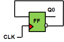
  • Johnson Counter enables us to design in such a manner that there is no combinatorial cell between any two registers. Let's have a look:
    Since the LSB i.e. Q0 toggles itself at every clock cycle, the 1-bit Johnson Counter can be used for Q0. Note that here we are using bit-by-bit synthesis instead of the conventional Karnaugh map approach to design our binary counter.

  • Similarly, higher order counter bits can be realized by higher order Johnson Counter, where the last bit would represent the binary counter bit. For Q1, the circuit would be:
  • The same can be extended in a recursive manner to design any n-bit binary counter.
  • Note that in this design, there is absolutely no combinatorial cells between any two registers, thereby making high operating speed possible.

    Time Period of the Clock T(clk-to-qbar),FF + Tsu,FF

    What is the trade-off here? The answer is dynamic power dissipation. Note that a conventional n-bit counter would use n flops. However, for the proposed design, 3-bit counter would need (1+2+4=) 7 flops, 4 bit counter would need (1+2+4+8=) 15 flops and so on. This design might find practical application for lower order counter widths like 4-6. 

    Above that, the design would dissipate too much power to be of any practical use.

July 12, 2013

Placement of Clock Gating Cells

Clock Gating Cells are indispensable components to save dynamic power. However, the backend design engineers must be prudent while placing them. In this post, I'll talk about the trade-off between timing and power that underlies the placement of clock gating cells.

Consider that your SoC has two IPs, and a single clock source. These two IPs are synchronous, and might work independently (i.e. without any interaction with the other IP) in some use-case of the chip. This entails the need of two clock gating cells. Now the question arises: where to place these clock gating cells. 
  • Near the sink, i.e. the clock source, or
  • Near the source, i.e. the respective IPs
Let's take up pros and cons of the two placement scenarios.


  1. Clock Gating Cells placed near the source: As shown in the figure, placing the clock gating cells near the clock source, can  the increase the uncommon clock path (shown in yellow). 


Recall from the post: Common Path Pessimism that while doing timing analysis, the effect of OCV derates come into picture for the uncommon clock path because the clock tree buffers in the uncommon path can behave differently and hence an STA engineer needs to take into account that extra uncertainty or pessimism while doing timing analysis. Such a scenario is therefore hostile to the timing engineers. However, from power perspective this scheme is quite favorable. Since as soon as the clock gate is turned "Off", all the clock buffers in the fanout of that clock gate are also "off" or in other words, they do not toggle and hence do not dissipate dynamic power. Like any engineering problem, there exists a trade-off between two conflicting factors, and designers often need to prioritize.

2. Clock Gating Cells placed near the sink: While this scenario, with greater common path as compared to the first scenario and hence making the timing easier to met, is not friendly from the power perspective. 
All the clock tree buffers  in the common clock path (shown tin red) lie before the clock gate and hence would always be "on" and keep on toggling at the clock frequency, thereby dissipating dynamic power.


Solution:
The pertinence of a solution is dictated on many factors. Permissible clock latencies, power dissipation specifications, timing closure challenges and also the use-case.

Let's say we had a requirement that IP 2 will function if and only if IP 1 is on. In this case we could have placed the clock gates in series like this:


By having the two clock gates in series, we would save the dynamic power of all the clock tree buffers in the fanout of first clock gate. Moreover, the uncommon path is significantly less as compared to the scenario 1.

Again note that this solution would not work if we had the use-case where IP 1 could be "off", while IP 2 still "on".