Showing posts with label DFT. Show all posts

April 24, 2018

False Path v/s Case Analysis v/s Disable Timing

Often people have asked me the difference between set_false_path, set_case_analysis and set_disable_timing. While the difference between these three is quite easy, it's the implications that leave many designers stumped.

Let me take a shot at explaining the difference.

1. FALSE PATH: All the timing paths which designers know won't be exercised on the fly, and they don't really need to meet any timing constraints on that path can be marked as false paths.
Tools would compute delays on all arcs on the false-path, would try to meet slopes/max-fanout/max-capacitance targets for all nodes along the path, but these paths would never surface up as timing (setup and hold) violations. However, if designers are too concerned about meeting slope and max cap targets, they usually prefer to mark such paths as set_multicycle_path instead.

Some examples of false path:

Consider the circuit above. The select line of the two multiplexers is complement of each other. STA tool, however, doesn't understand this logic and would treat all nodes as X (either 0 or 1). In practice, there can never be a timing path between 

C -> E -> G
D -> F -> G

And these can be marked as false paths.

2. CASE ANALYSIS: Using set_case_analysis, any node can be constrained to a boolean logic value of 1 or 0. All case values are evaluated and propagated through the design. For example, if one input of an AND gate is 0, 0 being the controlling value, the output of AND gate would also be 0 and this 0 is propagated downstream. The timing arcs for set_case_analysis are not evaluated and they never show up in the timing reports. However, PnR tooks would still fix max transition, max capacitance and max-fanout violations on these nets/pins.

  • Some latest tool versions also support a case value of static which means that the node will always be static (never toggle), and this is used to reduce the pessimism which doing noise analysis.
  • Case analysis is also particularly useful for DFT modes where you would want to set a few configuration registers and drive the chip into a particular DFT mode: like atspeed, shift or stuck-at mode. This acts as an additional level of verification because you'd expect to see only scan chains in the shift mode with scan enable being 1. You'd expect to see functional paths in the atspeed mode with scan enable being X, and you'd expect to see only paths ending at functional register inputs in the stuck-at mode with scan enable being 0.

3. DISABLE TIMING: This disables a particular timing arc, and that timing arc or any timing path through the disabled timing arc is not computed. This tends to be a bit disruptive as compared to false paths or case analysis, but in some cases this is indispensable and the easiest way to achieve the intent. For example if you have a MUX based divider which receives the clock signal at the select line of the multiplexer, and two functional enables at the multiplexer inputs, STA tool would try to propagate the clock to the output of the MUX via the MUX select line to the output. But for a MUX, a select line only controls what gets propagated to the output. In practice, there's no arc between select and output and should be disabled.
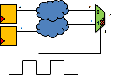


Both case analysis and disable timing result in fewer timing paths to be analyzed. False path still tries to fix the design rule (max cap, max transition and max fanout) violations.

April 21, 2013

Puzzle: DFT Shift Frequency

It is a well known fact that DFT Shifting is done at a slower frequency. Well, I'm gonna list down some cons against this. You'll have to tell the pros!

  • Lower is the frequency, greater is the test time. In modern SoCs, tester cost  (which is directly proportional to the tester time) accounts for roughly 40% of the selling price of a single chip. It would be pragmatic to decrease the test time by increasing the frequency. No?
  • Increasing the frequency would not pose any timing issue. Because, hold would anyway be met (Hold check is independent of frequency). And setup would never be in the critical path considering the fact that scan chains only involve direct path from output of a flop to scan input pin of the next flop, devoid of any logic.

Then why not test at a higher frequency, which is at least closer to the functional frequency? What could possibly be the reason for testing at slower frequency?

April 19, 2013

Puzzle: Stuck-At Fault

A brief introduction to Stuck-At Faults was given in the post: Design for Testability: Need for Modern VLSI Design. You might want to go through it first. Anyway, as the name suggests, stuck-at faults manifest themselves if any particular node  in the design is "stuck" at either 0 or 1. A plausible explanation for stuck-at-0 (SA0) might be that the particuular node on question has somehow been shorted to Ground (GND at 0V) . Similarly, a node might be Stuck-At-1 (SA1) if let's say it is somehow shorted to the VDD (at logic 1).

In order to detect a stuck-at-0 fault, we would try to excite that node to the opposite value, i.e. 1 and try and see if we are able to achieve that. If we are able to do so, we can safely say that the node in question in NOT stuck-at-0. And vice-versa.

In the below question, we intend to check the node X for a stuck-at-0 fault. Can you tell what input vector (A,B,C) would be need to give to do so?


Two Pillars of DFT: Controllability & Observability

I haven't given an equitable share of attention to DFT, and now, it's time to make some amends! Just like Timing is built on two pillars: Setup & Hold, entire DFT is built on two pillars: Controllability & Observablity.  Very often you would find DFT folks cribbing that they can't control a particular node, or don't have any mechanism to observe a particular node in question. You may like to review the previous post: DFT Modes: Perspective before proceeding further.

Shifting our attention to the pillars of DFT, let's define the two.
  • Controllability: It is the ability to have a desired value (which would be one out of 0 or 1) at any particular node of the design. If the DFT folks have that ability, they say that that particular node is 'controllable'. Which in turn means that they can force a value of either 0 or 1, on that node!
  • Observability: It is the ability to actually observe the value at a particular node whether it is 0 or 1 by forcing some pre-defined inputs. Note that, unlike the circuit that we make on paper, the SoC is a colossal design and one can observe a node only via the output ports. So, DFT folks actually need a mechanism to excite a node and then fish that value out of the SoC via some output port and then 'observe' it!
Ideally, it is desired to have each and every node of the design controllable and observable. But reality continues to ruin the life of DFT folks! (Source: Calvin & Hobbes). It is not always possible or rather practical to have all the nodes in a design under your control, because of the sheer complexity that modern SoCs possess. And therefore, it is the reason you would hear them talk about 'Coverage'. Let's say coverage is 99%, this means that we have the ability to control and observe 99% of the nodes in the design (A pretty big number, indeed!).

Now let's take some simple examples.
In the above example, if we have control the flops such that the combo cloud results in 1 at both the inputs of AND gate, we say that the node X is controllable for 1. Similarly, if we can control any input of AND gate for 0, we say that node X is controllable for 0. Similarly, let's say we wish to observe the output of FF1. If we can somehow replicate the value of FF1 by making the combo clouds and AND gate transparent to the value at FF1, we say that output of FF1 is observable. Intuition tells us that for AND gate to be transparent, we should have the controllability of other node for 1. Because when one input of AND gate is 1, whatever is the value at the other input, it is simply passed on!!

January 26, 2013

Lock-Up Latch: Implication on Timing

Lock-Up Latches are important elements for any STA engineer while closing timing on their DFT Modes: specially the Hold Timing Closure of the Shift Mode. While shifting, the scan chains come into picture, which are nothing but the chains of Flops involving the output pin of one flop, connected to the Scan-Input or Test-Input pin of the other flop, and so on, forming a chain. 

Now, imagine that we have two functionally asynchronous domains 1 and 2. Functionally asynchronous means that during the normal mode of operation (Functional Mode), the two domains do not interact with each other. However, very rarely do the designers have the liberty to make a separate scan chain for functionally asynchronous domains. Let's consider the following scenario: where domain 1 has the average clock latency of 3ns, and domain 2 has the average latency of 6ns. And the time period of the test clock is, let's say, 10ns.


Now, let's see the timing checks for this scenario. The output of the last flop of the domain 1 is in scan-chain and connected to the Test-Enable input of the first flop of domain 2. The check would be like: 

Owing to the positive clock skew, the setup check would be relaxed, but hold would be critical. Two possible options to fix the hold timing:
  • Insert the buffers, to add sufficient delay, so that hold is finally met.
  • To add the Lock-Up Latch between the two flops where scan chain crosses the functional domains.
The first might not be a robust solution because the delay of the buffers would vary across the PVT Corners and RC Corners. In the worse case, there might be a significant variation in the delays across corners and you might witness closure of timing in one corner, but violation in other corner!

Second solution is a more robust solution because it obviates the above scenario. Hence see how it does it.
 

Timing Check would be like:


Hence, both setup and hold checks are relaxed!!
[Please note that in the above circuit, the latch is a negative level triggered latch.]

January 17, 2013

DFT Modes: Perspective

As more number of transistors are finding their way onto a single SoC, Design for Testability (DFT) is becoming an increasing important function of the SoC design cycle. As the technology nodes are shrinking consistently, the probability of the occurrence of the faults is also increasing which makes DFT an indispensable function for modern sub-micron SoCs. What are the possible faults within an SoC and whhat all ways are possible to detect them? We will take them up briefly.

Imagine that you own a chip manufacturing company for the automotive industry. The end application can be something meant for infotainment, engine management, rear view camera, ethernet connectivity, power  glasses or for a critical application like collision detector or air-bag control etc. You wouldn't like to sell a faulty chip to your customers for two main reasons:
  • Trust of the customer which would impact the goodwill of the company.
  • Loss of business: Maybe because the customer opted for some other semiconductor vendor or even worse, the chip failed at the user end and he sued your customer who ultimately sued you!
Hence, it is pretty important to test the chip before shipping it out to the customers.

Types of fault and their detection:
  • Structural Fault: Basically refers to the faults due to faulty manufacturing at the fabs. Even a tiny dust particle has cause shorts or opens in an SoC. 
    Let's try to understand it from our example. Let's say you manufactured the chip but there is a fair probability  that there might be some structural inadequacies in the form of shorts or opens. Imagine any digital circuit. Single short or a single open can cause the entire functionality of the device to go haywire. Structural testing is done during the DFT tests or modes called as Shift and Stuck-At Capture. We'll discuss these in detail in the upcoming posts. Note that these tests are conducted after manufacturing, before shipping the part to the customer.
  • Transition Faults: Signal transitions are nothing but the voltage levels while they switch from either 'high' to 'low' or vice-versa. There is a designated time before the clock edge when all the signals should be stable at the input of the Flop (a very crude definition of setup time) and also a designated time after the clock edge when none of the signals should change their states at the input of the Flop (a very crude definition of hold time). Any such fault in the transition times (conversely: setup or hold violations) is referred to as a transition fault.

    Going back to our example. Suppose that you first filtered out the chips which had some structural fault. Now you would test the remaining chips for transition faults. What would happen if you ship a chip with a transition fault to a customer? If it had a setup violation, the chip will not be able to work at the specified frequency. However, it will be able to work at a slower frequency. If it had a hold violation, the chip will not be able to work at all! One possible consequence from our example could be that in an event of a collision you would expect a few micro- or nano- seconds for the air bag to open up, it might ending up taking seconds! Unfortunately, it would be too late.
    The At-Speed test is used to screen the chip for transition faults.


    Broadly speaking, there are only two types of the faults as discussed above. However, there's another possibility which can arise. 

    Imagine that your car has an SoC which senses a collision and opens the  air bag  within a few micro-seconds of the collision. You would expect it to open up if such a scenario arises. But what if your car is, let's say, 6 years old and the chip is now not functioning as expected. In this case, you would like to test the chip first. And if it is fine, you may proceed on to ignite the engine and start the car. Such a scenario would demand conducting a test while the chip is in operation. Such a DFT test is called LBIST Test (Logical-Built-in-Self Test). In an LBIST test, one would be testing the entire chip or a sub-part of it for structural and/or transition faults. Such a test for memory is referred to as MBIST Test (Memory-Built-in-Self-Test).

    An important characteristic of a built in self test is that it is self sufficient. It would carry out the test internally, following a software trigger, without any external input; carry the test; and send out a signature in terms of PASS/FAIL.

    A failed LBIST test on the air-bag chip, might flash a warning and can prevent the user from starting the car engine! It might sound cruel, but it can surely save your life!!

    In the upcoming posts, we would discuss these from the design perspective. Stay tuned!

July 28, 2012

Design for Testability: The Need for Modern VLSI Design

DFT is the acronym for Design for Testability. DFT is an important branch of VLSI design and in crude terms, it involves putting up a test structure on the chip itself to later assist while testing the device for various defects before shipping the part to the customer.

Have you ever wondered how the size of electronic devices is shrinking? Mobile phone used to be big and heavy with basic minimal features back in 90s. But nowadays, we have sleek phones, lighter in weight and with all sorts of features from camera, bluetooth, music player and not to forget with faster processors. All that's possible because of the scaling of technology nodes. Technology node refers to the channel length of the transistors which form the constituents of your device. Well, we are moving to reduced channel lengths. Some companies are working on technology nodes as small as 18nm. Smaller is the channel length, more difficult it is for the foundries to manufacture. And more are the chances of manufacturing faults.

Possible manufacturing faults are: Opens and shorts.
The figure shows two metal lines one of which got "open" while other got "shorted". As we are moving to lower technology nodes, not only the device size is shrinking but that also enables to pack more transistors on the same chip and hence density is increasing. And manufacturing faults have become therefore indispensable. DFT techniques enable us to test these (other kinds as well) faults.